Next: Software Previous: Installation
Electrical Subsystems
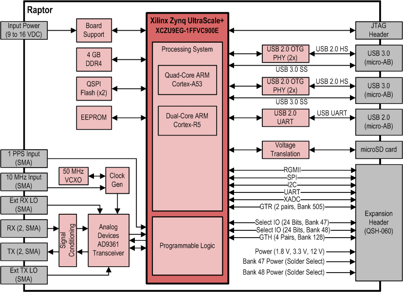
This section describes the major electrical components of the Raptor board. Figure 6 show a block diagram of all the main components of the Raptor SDR.
Xilinx Zynq UltraScale+ MPSOC
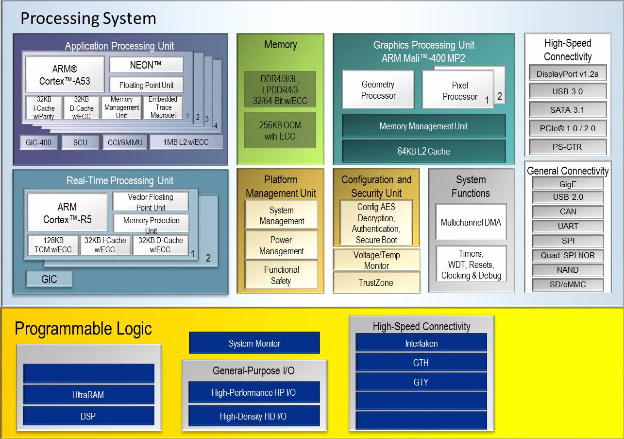
The Raptor SDR includes a Xilinx Zynq UltraScale+ XCZU9EG-1FFVC900E FPGA. The processing system in a Zynq Ultrascale+ MPSOC features the ARM flagship Cortex-A53 64 bit quad-core processor and Cortex-R5 dual-core real-time processor, and a single Mali-400 graphics processing unit (GPU) with pixel and geometry processor and 644 KB L2 cache. All SOM memory and digital interfaces connect to the Zynq through the Processing System (PS) or Programmable Logic (PL). The Analog Devices AD9361 RF transceiver is connected through the Zynq Ultrascale+ PL.
Source: Xilinx, Inc.
For more information, refer to the Zynq UltraScale site [1].
Analog Devices AD9361 Transceiver
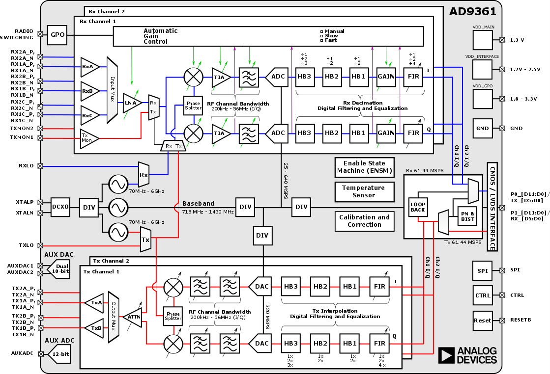
The Raptor SDR includes Analog Devices AD9361 RF Agile Transceiver. The AD9361 is a high performance, highly integrated radio frequency (RF) Agile Transceiver™ designed for use in 3G and 4G base station applications. Its programmability and wideband capability make it ideal for a broad range of transceiver applications. The device combines a RF front end with a flexible mixed-signal baseband section and integrated frequency synthesizers, simplifying design-in by providing a configurable digital interface to a processor. The AD9361 receiver LO operates from 70 MHz to 6.0 GHz and the transmitter LO operates from 47 MHz to 6.0 GHz range, covering most licensed and unlicensed bands. Channel bandwidths from less than 200 kHz to 56 MHz are supported.
Source: © by Analog Devices, Inc. (ADI), May 2017. Reproduced with permission from ADI.
For more information, refer to the AD9361 site [2].
Analog Filters
Transmit Path
The transmitter section consists of two identical and independently controlled channels that provide all digital processing, mixed signal, and RF blocks necessary to implement a direct conversion system while sharing a common frequency synthesizer. The digital data received from the Baseband Processors (BBP) passes through a fully programmable 128-tap FIR filter with interpolation options. The FIR output is sent to a series of interpolation filters that provide additional filtering and data rate interpolation prior to reaching the DAC. Each 12-bit DAC has an adjustable sampling rate. Both the I and Q channels are fed to the RF block for upconversion.
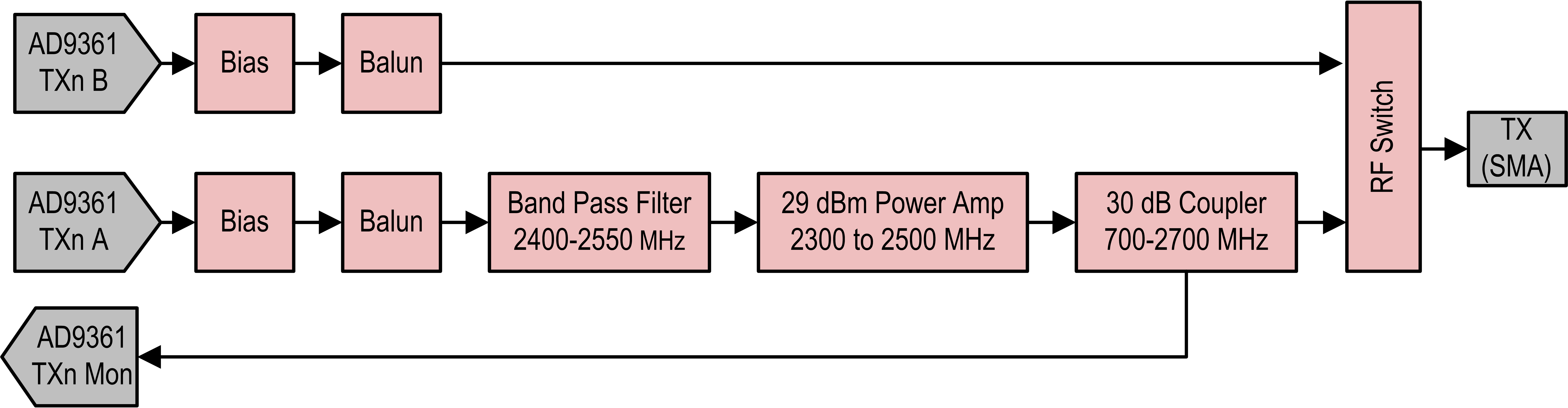
The Raptor SDR includes two identical transmit ports. Each transmit port has 2 channels A and B .
Channel A contains a band pass filter with a frequency range of 2400 MHz to 2550 MHz and then it passes through an MGA-43228 power amplifier.MGA-43228 is a power amplifier for use in the (2.3-2.5)GHz band.
MGA-43228 Specifications :
- High gain: 38.5dB
- Low gain: 14.9dB
- High linearity performance: 29.2dBm at 5V supply (2.5% EVM, 64-QAM 3⁄4 FEC rate OFDMA, 10MHz bandwidth)
The power amplifier can operate in low gain or high gain mode and this setting is configurable through the AD9361 general purpose output 3 (GPO_3) pin. The power amplifier can be bypassed/enabled through GPO_2 pin.
Channel B is bypass channel.The figure below shows a simplified illustration of the transmit path and the ways it can be configured.
| TX Power Amplifier Control | GPO_2 |
|---|---|
| Power Amplifier Bypassed | 0 |
| Power Amplifier Enabled | 1 |
| TX Power Amplifier Control | GPO_3 |
|---|---|
| Full-Gain Mode (38.5 dB) | 0 |
| Low-Gain Mode (14.9 dB) | 1 |
Receive Path
The receiver path contains two independently controlled channels that can receive signals from different sources, allowing the device to be used in multiple input, multiple output (MIMO) systems while sharing a common frequency synthesizer. Each channel has three inputs that can be multiplexed to the signal chain, making the AD9361 suitable for use in diversity systems with multiple antenna inputs. The receiver is a direct conversion system that contains a low noise amplifier (LNA), followed by matched in-phase (I) and quadrature (Q) amplifiers, mixers, and band shaping filters that down convert received signals to baseband for digitization. External LNAs can also be interfaced to the device, allowing designers the flexibility to customize the receiver front end for their specific application.
The Raptor SDR receive path contains four-band pre-selector per receiver channel that are run-time configurable by using the GPO_0 and GPO_1 bits. The Figure below shows a high level diagram of the receive path.
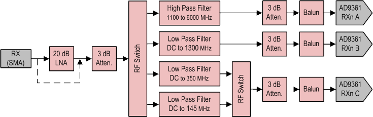
The following table explains the GPO configuration needed to select each filter.
| RX Filter Selection | Part Number | GPO_1 | GPO_0 |
|---|---|---|---|
| 1100 to 6000 | MHz HFCN-1100+ | 0 | 0 |
| DC to 1300 MHz | LFCN-1000+ | 0 | 1 |
| DC to 350 MHz | LFCN-225+ | 1 | 0 |
| DC to 145 MHz | LFCN-80+ | 1 | 1 |
Memory
DDR4
The Raptor board includes four Micron MT40A512M16HA-083E DDR4-2400 memory components, totaling 4GB of random access memory. The DDR4 memory is wired to the Zynq Ultrascale+ DDRC hard memory controller. DDR4 connections between Zynq Ultrascale+ DDRC hard memory controller and memory components are shown in the table below.
| XCZU9EG Pin | Net Name | U50, U51,U52,U53 | |
|---|---|---|---|
| Ball Number | Pin Name (U#) | ||
| AK25 | PS_DDR4_A0 | P3 | A0 (U*) |
| AK28 | PS_DDR4_A1 | P7 | A1 (U*) |
| AK27 | PS_DDR4_A2 | R3 | A2 (U*) |
| AH24 | PS_DDR4_A3 | N7 | A3 (U*) |
| AK24 | PS_DDR4_A4 | N3 | A4 (U*) |
| AJ30 | PS_DDR4_A5 | P8 | A5 (U*) |
| AE22 | PS_DDR4_A6 | P2 | A6 (U*) |
| AE25 | PS_DDR4_A7 | R8 | A7 (U*) |
| AE23 | PS_DDR4_A8 | R2 | A8 (U*) |
| AE24 | PS_DDR4_A9 | R7 | A9 (U*) |
| AD22 | PS_DDR4_A10 | M3 | A10/AP (U*) |
| AH23 | PS_DDR4_A11 | T2 | A11(U*) |
| AF21 | PS_DDR4_A12 | M7 | A12/BC_n (U*) |
| AG21 | PS_DDR4_A13 | T8 | A13 (U*) |
| AF22 | PS_DDR4_A14 | L2 | A14/WE_n (U*) |
| AF23 | PS_DDR4_A15 | M8 | A15/CAS_n (U*) |
| AD21 | PS_DDR4_A16 | L8 | A16/RAS_n (U*) |
| AG26 | PS_DDR4_BA0 | N2 | BA0 (U*) |
| AF25 | PS_DDR4_BA1 | N8 | BA1 (U*) |
| AF26 | PS_DDR4_BG0 | M2 | BG0 (U*) |
| AK22 | PS_DDR4_DQ0 | A3 | DQU0 (U50) |
| AH17 | PS_DDR4_DQ1 | C8 | DQU5 (U50) |
| AJ17 | PS_DDR4_DQ2 | D7 | DQU7 (U50) |
| AH16 | PS_DDR4_DQ3 | B8 | DQU1 (U50) |
| AK15 | PS_DDR4_DQ4 | C3 | DQU2 (U50) |
| AK14 | PS_DDR4_DQ5 | C7 | DQU3 (U50) |
| AJ14 | PS_DDR4_DQ6 | D3 | DQU6 (U50) |
| AH14 | PS_DDR4_DQ7 | C2 | DQU4 (U50) |
| AK16 | PS_DDR_DM0 | E2 | DMU_n/DBIU_n (U50) |
| AJ15 | PS_DDR_DQS_P0 | B7 | DQSU_p (U50) |
| AJ16 | PS_DDR_DQS_N0 | A7 | DQSU_n (U50) |
| AK19 | PS_DDR4_DQ8 | J7 | DQL7 (U50) |
| AK18 | PS_DDR4_DQ9 | J3 | DQL6 (U50) |
| AJ19 | PS_DDR4_DQ10 | H8 | DQL5 (U50) |
| AH19 | PS_DDR4_DQ11 | F7 | DQL1 (U50) |
| AK21 | PS_DDR4_DQ12 | H2 | DQL4 (U50) |
| AK22 | PS_DDR4_DQ13 | G2 | DQL0 (U50) |
| AH21 | PS_DDR4_DQ14 | H7 | DQL3 (U50) |
| AJ22 | PS_DDR4_DQ15 | H3 | DQL2 (U50) |
| AK20 | PS_DDR_DM1 | E7 | DML_n/DBIL_n (U50) |
| AJ20 | PS_DDR_DQS_P1 | G3 | DQSL_p (U50) |
| AJ21 | PS_DDR_DQS_N1 | F3 | DQSL_n (U50) |
| AG14 | PS_DDR4_DQ16 | C8 | DQU5 (U51) |
| AG15 | PS_DDR4_DQ17 | B8 | DQU1 (U51) |
| AG16 | PS_DDR4_DQ18 | D7 | DQU7 (U51) |
| AF16 | PS_DDR4_DQ19 | C7 | DQU3 (U51) |
| AD14 | PS_DDR4_DQ20 | A3 | DQU0 (U51) |
| AD16 | PS_DDR4_DQ21 | D3 | DQU6 (U51) |
| AD15 | PS_DDR4_DQ22 | C3 | DQU2 (U51) |
| AD17 | PS_DDR4_DQ23 | C2 | DQU4(U51) |
| AE14 | PS_DDR_DM2 | E2 | DMU_n/DBIU_n (U51) |
| AE15 | PS_DDR_DQS_P2 | B7 | DQSU_p (U51) |
| AF15 | PS_DDR_DQS_N2 | A7 | DQSU_n (U51) |
| AE17 | PS_DDR4_DQ24 | J3 | DQL6 (U51) |
| AE18 | PS_DDR4_DQ25 | H8 | DQL5 (U51) |
| AE20 | PS_DDR4_DQ26 | F7 | DQL1 (U51) |
| AE19 | PS_DDR4_DQ27 | H7 | DQL3 (U51) |
| AG18 | PS_DDR4_DQ28 | H3 | DQL2 (U51) |
| AH18 | PS_DDR4_DQ29 | H2 | DQL4 (U51) |
| AG19 | PS_DDR4_DQ30 | G2 | DQL0 (U51) |
| AG20 | PS_DDR4_DQ31 | J7 | DQL7 (U51) |
| AF20 | PS_DDR_DM3 | E7 | DML_n/DBIL_n (U51) |
| AF17 | PS_DDR_DQS_P3 | G3 | DQSL_p (U51) |
| AF18 | PS_DDR_DQS_N3 | F3 | DQSL_n (U51) |
| Y24 | PS_DDR4_DQ32 | D7 | DQU7 (U52) |
| Y25 | PS_DDR4_DQ33 | B8 | DQU1 (U52) |
| AA25 | PS_DDR4_DQ34 | C8 | DQU5 (U52) |
| AA26 | PS_DDR4_DQ35 | C7 | DQU3 (U52) |
| AC26 | PS_DDR4_DQ36 | A3 | DQU0 (U52) |
| AD24 | PS_DDR4_DQ37 | D3 | DQU6 (U52) |
| AD25 | PS_DDR4_DQ38 | C2 | DQU4 (U52) |
| AC24 | PS_DDR4_DQ39 | C3 | DQU2 (U52) |
| AB26 | PS_DDR_DM4 | E2 | DMU_n/DBIU_n (U52) |
| AB24 | PS_DDR_DQS_P4 | B7 | DQSU_p (U52) |
| AB25 | PS_DDR_DQS_N4 | A7 | DQSU_n (U52) |
| W27 | PS_DDR4_DQ40 | A3 | DQU0 (U53) |
| W26 | PS_DDR4_DQ41 | C8 | DQU5 (U53) |
| W24 | PS_DDR4_DQ42 | D3 | DQU6 (U53) |
| W25 | PS_DDR4_DQ43 | C2 | DQU4 (U53) |
| U26 | PS_DDR4_DQ44 | D7 | DQU7 (U53) |
| U27 | PS_DDR4_DQ45 | C7 | DQU3 (U53) |
| U25 | PS_DDR4_DQ46 | B8 | DQU1 (U53) |
| U24 | PS_DDR4_DQ47 | C3 | DQU2 (U53) |
| V24 | PS_DDR_DM5 | E2 | DMU_n/DBIU_n (U53) |
| V26 | PS_DDR_DQS_P5 | B7 | DQSU_p (U53) |
| V27 | PS_DDR_DQS_N5 | A7 | DQSU_n (U53) |
| AA30 | PS_DDR4_DQ48 | G2 | DQL0 (U52) |
| AB29 | PS_DDR4_DQ49 | H3 | DQL2 (U52) |
| AB30 | PS_DDR4_DQ50 | H2 | DQL4 (U52) |
| AB28 | PS_DDR4_DQ51 | F7 | DQL1 (U52) |
| AC27 | PS_DDR4_DQ52 | H7 | DQL3 (U52) |
| AD27 | PS_DDR4_DQ53 | H8 | DQL5 (U52) |
| AD29 | PS_DDR4_DQ54 | J3 | DQL6 (U52) |
| AD30 | PS_DDR4_DQ55 | J7 | DQL7 (U52) |
| AC30 | PS_DDR_DM6 | E7 | DML_n/DBIL_n (U52) |
| AC28 | PS_DDR_DQS_P6 | G3 | DQSL_p (U52) |
| AC29 | PS_DDR_DQS_N6 | F3 | DQSL_n (U52) |
| AA28 | PS_DDR4_DQ56 | G2 | DQL0 (U53) |
| AA27 | PS_DDR4_DQ57 | J7 | DQL7 (U53) |
| Y28 | PS_DDR4_DQ58 | H8 | DQL5 (U53) |
| Y27 | PS_DDR4_DQ59 | J3 | DQL6 (U53) |
| W30 | PS_DDR4_DQ60 | H3 | DQL2 (U53) |
| V30 | PS_DDR4_DQ61 | F7 | DQL1 (U53) |
| V28 | PS_DDR4_DQ62 | H7 | DQL3 (U53) |
| V29 | PS_DDR4_DQ63 | H2 | DQL4 (U53) |
| Y30 | PS_DDR_DM7 | E7 | DML_n/DBIL_n (U53) |
| W29 | PS_DDR_DQS_P7 | G3 | DQSL_p (U53) |
| Y29 | PS_DDR_DQS_N7 | F3 | DQSL_n (U53) |
| AJ24 | PS_DDR_CS_N | L7 | ACT_n (U*) |
| AJ25 | PS_DDR_CKE | K2 | CKE (U*) |
| AJ29 | PS_DDR_ODT | K3 | ODT (U*) |
| AJ26 | PS_DDR_CK_P | K7 | CK_p (U*) |
| AJ27 | PS_DDR_CK_N | K8 | CK_n (U*) |
| AC14 | PS_DDR_PARITY | T3 | PAR (U*) |
| AD19 | PS_DDR_ALERT | P9 | ALERT_n (U*) |
| AC16 | PS_DDR_RAM_RST_N | P1 | RESET_n (U*) |
Notes:
- U* - All memory components share the same connection.
On-chip Memory
The Xilinx Zynq UltraScale+ has 256 KB of on-chip memory (OCM) RAM. Accesses to the OCM must pass through the OCM protection unit, OCM_XMPU. The entire 256 KB of RAM is divided into 64 blocks (4 KB each) and assigned security attributes independently.
Quad SPI Flash
Raptor SDR includes dual Micron MT25QU512ABB8E12 serial NOR flash Quad-SPI memories that are capable of holding the boot image of the MPSoC system. To achieve higher performance two Quad-SPI devices are connected in parallel and provide an 8-bit data bus for booting and configuration.
The dual Quad-SPI flash memory located at U37/U39 provide 1 Gbit of non-volatile storage that can be used for booting, configuration and data storage. The connections between the flash memory and the XCZU9EG MPSoC are shown in the table below.
| XCZU9EG Pin | Net Name | Quad-SPI U37(LWR), U38 (UPR) | |
|---|---|---|---|
| Ball Number | Pin Name (U#) | ||
| G18 | MIO4_QSPI_LWR_DQ0 | D3 | DQ0 |
| H17 | MIO1_QSPI_LWR_DQ1 | D2 | DQ1 |
| E18 | MIO2_QSPI_LWR_DQ2 | C4 | W#/DQ2 |
| F18 | MIO3_QSPI_LWR_DQ3 | D4 | DQ3/RESET#/HOLD# |
| C18 | MIO0_QSOI_LWR_CLK | B2 | C |
| J17 | MIO5_QSPI_LWR_CS_n | C2 | S# |
| K18 | MIO8_QSPI_UPR_DQ0 | D3 | DQ0 |
| I18 | MIO9_QSPI_UPR_DQ1 | D2 | DQ1 |
| B18 | MIO10_QSPI_UPR_DQ2 | C4 | W#/DQ2 |
| G19 | MIO11_QSPI_UPR_DQ3 | D4 | DQ3/RESET#/HOLD# |
| K17 | MIO12_QSPI_UPR_CLK | B2 | C |
| A18 | MIO7_QSPI_UPR_CS_n | C2 | S# |
The table below shows the QSPI boot modes that the Raptor SDR support.
| PS BOOT Mode | SW1-2 | SW1-1 |
|---|---|---|
| QSPI(32-bit Addressing) | OFF | ON |
| QSPI(24-bit Addressing) | ON | OFF |
The configuration and Quad-SPI sections of the Zynq Ultrascale+ MPSoC Technical Reference Manual (UG1085) provide more details on using Quad-SPI. For more details about the Micron MT25QU512ABB8E12 see the datasheet at the Micron website.
EEPROM
The Raptor SDR includes a M24256-DFDW6 EEPROM. The M24256 is a 256-Kbit I2C compatible EEPROM organized as 32K x 8 bits and it operates with a supply voltage of 1.8 V. The connections between the flash memory and the XCZU9EG MPSoC are shown in the table below.
| Signal | Description | Zynq Bank | MIO | U38 Pin |
|---|---|---|---|---|
| E0 | Chip Enable | N/A | N/A | 1 |
| E1 | Chip Enable | N/A | N/A | 2 |
| E2 | Chip Enable | N/A | N/A | 3 |
| WC | Write Control | N/A | N/A | 7 |
| VCC | Supply Voltage | N/A | N/A | 8 |
| SCL | Serial Clock | MIO Bank 500 | 16 | 6 |
| SDA | Serial Data | MIO Bank 500 | 17 | 5 |
| VSS | Ground | N/A | N/A | 4 |
Micro SD
The Raptor board includes a secure digital input/output(SDIO) interface to provide access to general purpose non-volatile SDIO memory cards and peripherals.The Raptor SD card interface supports the SD1 configuration boot mode documented in the Zynq UltraScale+ MPSoC Technical Reference Manual (UG1085).
Interface
| Signal | Description | Zynq Bank | MIO | J9 Pin |
|---|---|---|---|---|
| PS_SDIO_WP | Write Protect | MIO Bank 500 | 44 | |
| PS_SDIO_CD_n | MIO Bank 500 | 45 | 10 | |
| PS_SDIO_DATA0 | Data bit 0 | MIO Bank 500 | 46 | 7 |
| PS_SDIO_DATA1 | Data bit 1 | MIO Bank 500 | 47 | 8 |
| PS_SDIO_DATA2 | Data bit 2 | MIO Bank 500 | 48 | 1 |
| PS_SDIO_DATA3 | Data bit 3 | MIO Bank 500 | 49 | 2 |
| PS_SDIO_CMD | Command bit | MIO Bank 500 | 50 | 3 |
| PS_SDIO_CLK | Clock | MIO Bank 500 | 51 | 5 |
| PS BOOT Mode | SW1-2 | SW1-1 |
|---|---|---|
| Micro SD | OFF | OFF |
Installing and removing the microSD Card
The microSD card slides into a spring-loaded slot on the back of the Raptor board.
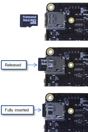
To install the card:
- Power off the Raptor board.
- Align the microSD card with the print facing up and the smallest edge toward the slot.
- Use your fingertip to gently slide the card into the slot. When you feel some resistance, gently press the card a little farther until you hear a click, which indicates the spring-lock engaged.
- Remove your finger from the card, which will spring out slightly to the fully inserted position. If the card springs out to the released position, press it in again until it remains in the fully inserted position.
To remove the card:
- Power off the Raptor board.
- Gently press the card into the slot with your fingertip until you hear a click, which indicates the spring-lock released.
- From the released position, slide the card away from the board.
USB 2.0/3.0 Host Device
The Zynq® UltraScale+™ MPSoC USB 3.0 controller consists of two independent dual-role device (DRD) controllers. The Raptor SDR includes 2 USB ports that can be individually configured to work as host or device at any given time.
USB 2.0/3.0 Host Device Port 0
The table below shows the pin assignments for USB port 0.
| Signal | Description | Zynq Bank | MIO | J10 Pin |
|---|---|---|---|---|
| REFCLCK | USB Clock | MIO Bank 502 | 52 | N/A |
| DIR | ULPI Dir output | MIO Bank 502 | 53 | N/A |
| NXT | ULPI NXT output | MIO Bank 502 | 55 | N/A |
| STP | ULPI STP input | MIO Bank 502 | 58 | N/A |
| Data[7:0] | USB data lines | MIO Bank 502 | [63-59,54,57,56] | N/A |
| RESET_B | Reset | MIO Bank 503 | PS_POR_B | N/A |
| REFSEL[2:0] | USB Chip select | N/A | N/A | N/A |
| DP | DP pin of USB | N/A | N/A | 3 |
| DM | DM Pin of USB | N/A | N/A | 2 |
| ID | Identification pin | N/A | N/A | 4 |
| CPEN | 5v external Vbus power | N/A | N/A | 1 |
| SSRX | Super Speed receive lines | PSGTR Bank 505 | PS_MGTRRXP2 | 9,10 |
| SSTX | Super Speed transmit lines | PSGTR Bank 505 | PS_MGTRRXP2 | 6,7 |
USB 2.0/3.0 Host Device Port 1
The table below shows the pin assignments for USB port 1.
| Signal | Description | Zynq Bank | MIO | J11 Pin |
|---|---|---|---|---|
| REFCLCK | USB Clock | MIO Bank 502 | 64 | N/A |
| DIR | ULPI Dir output | MIO Bank 502 | 65 | N/A |
| NXT | ULPI NXT output | MIO Bank 502 | 67 | N/A |
| STP | ULPI STP input | MIO Bank 502 | 70 | N/A |
| Data[7:0] | USB data lines | MIO Bank 502 | [75-71,66,69,68] | N/A |
| RESET_B | Reset | MIO Bank 503 | PS_POR_B | N/A |
| REFSEL[2:0] | USB Chip select | N/A | N/A | N/A |
| DP | DP pin of USB | N/A | N/A | 3 |
| DM | DM Pin of USB | N/A | N/A | 2 |
| ID | Identification pin | N/A | N/A | 4 |
| CPEN | 5v external Vbus power | N/A | N/A | 1 |
| SSRX | Super Speed receive lines | PSGTR Bank 505 | PS_MGTRRXP3 | 9,10 |
| SSTX | Super Speed transmit lines | PSGTR Bank 505 | PS_MGTRRXP3 | 6,7 |
IO
User LEDs
The following tables summarize bank and signal assignments for the USER LEDs.
| Signal | PL Bank | Pin |
|---|---|---|
| USER_LED0_R_n (RED) | ZynqMP PL - Bank 65 | AF13 |
| USER_LED0_G_n (GREEN) | ZynqMP PL - Bank 65 | AE13 |
| USER_LED0_B_n (BLUE) | ZynqMP PL - Bank 65 | AE12 |
| USER_LED1_R_n (RED) | ZynqMP PL - Bank 65 | AD12 |
| USER_LED1_G_n (GREEN) | ZynqMP PL - Bank 65 | AC13 |
| USER_LED1_B_n (BLUE) | ZynqMP PL - Bank 65 | AB12 |
Expansion Header
The following tables summarize bank and signal assignments on the J14 connector.
| Signal | Source | Pin |
|---|---|---|
| PSGTR_RX0_p | ZynqMP PS - Bank 505 | 2 |
| PSGTR_RX0_n | ZynqMP PS - Bank 505 | 4 |
| PSGTR_TX0_p | ZynqMP PS - Bank 505 | 6 |
| PSGTR_TX0_n | ZynqMP PS - Bank 505 | 8 |
| PSGTR_RX1_p | ZynqMP PS - Bank 505 | 14 |
| PSGTR_RX1_n | ZynqMP PS - Bank 505 | 16 |
| PSGTR_TX1_p | ZynqMP PS - Bank 505 | 20 |
| PSGTR_TX1_n | ZynqMP PS - Bank 505 | 22 |
| PS_SPI1_MOSI | ZynqMP PS - Bank 500 | 26 |
| PS_SPI1_MISO | ZynqMP PS - Bank 500 | 28 |
| PS_SPI1_CS1_n | ZynqMP PS - Bank 500 | 30 |
| PSG_SPI1_CLK | ZynqMP PS - Bank 500 | 32 |
| PS_UART1_TX | ZynqMP PS - Bank 500 | 36 |
| PS_UART1_RX | ZynqMP PS - Bank 500 | 38 |
| VCC_I2C1_SDA | ZynqMP PS - Bank 500 | 40 |
| VCC_I2C1_SCL | ZynqMP PS - Bank 500 | 42 |
| VCC_1V8 | Carrier | 44 |
| PS_MDC | ZynqMP PS - Bank 502 | 46 |
| PS_MDIO | ZynqMP PS - Bank 502 | 48 |
| PS_RGMII_TXD0 | ZynqMP PS - Bank 501 | 50 |
| PS_RGMII_TXD1 | ZynqMP PS - Bank 501 | 52 |
| PS_RGMII_TXD2 | ZynqMP PS - Bank 501 | 54 |
| PS_RGMII_TXD3 | ZynqMP PS - Bank 501 | 56 |
| PS_RGMII_TX_CTL | ZynqMP PS - Bank 501 | 58 |
| PS_RGMII_TXC | ZynqMP PS - Bank 501 | 60 |
| PS_RGMII_RXD0 | ZynqMP PS - Bank 501 | 49 |
| PS_RGMII_RXD1 | ZynqMP PS - Bank 501 | 51 |
| PS_RGMII_RXD2 | ZynqMP PS - Bank 501 | 53 |
| PS_RGMII_RXD3 | ZynqMP PS - Bank 501 | 55 |
| PS_RGMII_RX_CTL | ZynqMP PS - Bank 501 | 57 |
| PS_RGMII_RXC | ZynqMP PS - Bank 501 | 59 |
| PLGTH_RX0_n | ZynqMP PL - Bank 128 | 43 |
| PLGTH_RX0_p | ZynqMP PL - Bank 128 | 45 |
| PLGTH_TX0_n | ZynqMP PL - Bank 128 | 37 |
| PLGTH_TX0_p | ZynqMP PL - Bank 128 | 39 |
| PLGTH_RX1_n | ZynqMP PL - Bank 128 | 31 |
| PLGTH_RX1_p | ZynqMP PL - Bank 128 | 33 |
| PLGTH_TX1_n | ZynqMP PL - Bank 128 | 25 |
| PLGTH_TX1_p | ZynqMP PL - Bank 128 | 27 |
| PLGTH_RX2_n | ZynqMP PL - Bank 128 | 19 |
| PLGTH_RX2_p | ZynqMP PL - Bank 128 | 21 |
| PLGTH_TX2_n | ZynqMP PL - Bank 128 | 13 |
| PLGTH_TX2_p | ZynqMP PL - Bank 128 | 15 |
| PLGTH_RX3_n | ZynqMP PL - Bank 128 | 7 |
| PLGTH_RX3_p | ZynqMP PL - Bank 128 | 9 |
| PLGTH_TX3_n | ZynqMP PL - Bank 128 | 1 |
| PLGTH_TX3_p | ZynqMP PL - Bank 128 | 3 |
| PL47_IO0 | ZynqMP PL - Bank 47 | 61 |
| PL47_IO1 | ZynqMP PL - Bank 47 | 63 |
| PL47_IO2 | ZynqMP PL - Bank 47 | 65 |
| PL47_IO3 | ZynqMP PL - Bank 47 | 67 |
| PL47_IO4 | ZynqMP PL - Bank 47 | 69 |
| PL47_IO5 | ZynqMP PL - Bank 47 | 71 |
| PL47_IO6 | ZynqMP PL - Bank 47 | 73 |
| PL47_IO7 | ZynqMP PL - Bank 47 | 75 |
| PL47_IO8 | ZynqMP PL - Bank 47 | 79 |
| PL47_IO9 | ZynqMP PL - Bank 47 | 81 |
| PL47_IO10 | ZynqMP PL - Bank 47 | 83 |
| PL47_IO11 | ZynqMP PL - Bank 47 | 85 |
| PL47_IO12 | ZynqMP PL - Bank 47 | 87 |
| PL47_IO13 | ZynqMP PL - Bank 47 | 89 |
| PL47_IO14 | ZynqMP PL - Bank 47 | 91 |
| PL47_IO15 | ZynqMP PL - Bank 47 | 93 |
| PL47_IO16 | ZynqMP PL - Bank 47 | 97 |
| PL47_IO17 | ZynqMP PL - Bank 47 | 99 |
| PL47_IO18 | ZynqMP PL - Bank 47 | 101 |
| PL47_IO19 | ZynqMP PL - Bank 47 | 103 |
| PL47_IO20 | ZynqMP PL - Bank 47 | 105 |
| PL47_IO21 | ZynqMP PL - Bank 47 | 107 |
| PL47_IO22 | ZynqMP PL - Bank 47 | 109 |
| PL47_IO23 | ZynqMP PL - Bank 47 | 111 |
| VCC_PL47 | ZynqMP PL - Bank 47 | 77,95 |
| PL48_IO0 | ZynqMP PL - Bank 48 | 62 |
| PL48_IO1 | ZynqMP PL - Bank 48 | 64 |
| PL48_IO2 | ZynqMP PL - Bank 48 | 66 |
| PL48_IO3 | ZynqMP PL - Bank 48 | 68 |
| PL48_IO4 | ZynqMP PL - Bank 48 | 70 |
| PL48_IO5 | ZynqMP PL - Bank 48 | 72 |
| PL48_IO6 | ZynqMP PL - Bank 48 | 74 |
| PL48_IO7 | ZynqMP PL - Bank 48 | 76 |
| PL48_IO8 | ZynqMP PL - Bank 48 | 80 |
| PL48_IO9 | ZynqMP PL - Bank 48 | 82 |
| PL48_IO10 | ZynqMP PL - Bank 48 | 84 |
| PL48_IO11 | ZynqMP PL - Bank 48 | 86 |
| PL48_IO12 | ZynqMP PL - Bank 48 | 88 |
| PL48_IO13 | ZynqMP PL - Bank 48 | 90 |
| PL48_IO14 | ZynqMP PL - Bank 48 | 92 |
| PL48_IO15 | ZynqMP PL - Bank 48 | 94 |
| PL48_IO16 | ZynqMP PL - Bank 48 | 98 |
| PL48_IO17 | ZynqMP PL - Bank 48 | 100 |
| PL48_IO18 | ZynqMP PL - Bank 48 | 102 |
| PL48_IO19 | ZynqMP PL - Bank 48 | 104 |
| PL48_IO20 | ZynqMP PL - Bank 48 | 106 |
| PL48_IO21 | ZynqMP PL - Bank 48 | 108 |
| PL48_IO22 | ZynqMP PL - Bank 48 | 110 |
| PL48_IO23 | ZynqMP PL - Bank 48 | 112 |
| VCC_PL48 | ZynqMP PL - Bank 48 | 78,96 |
| VCC_3V3 | Carrier | 113 |
| VCC_3V3 | Carrier | 115 |
| VCC_9V_to_16V | Carrier | 114 |
| SYSMON_V_p | ZynqMP XADC Interface | 117 |
| SYSMON_V_n | ZynqMP XADC Interface | 119 |
| PS_POR_n | 118 | |
| EXP_PRSNT_n | 120 |
Reset Sources
ZynqMP Power‐on Reset (PS_POR_B)
Depressing and then releasing pushbutton SW2 causes net PS_POR_B to strobe Low. This reset is used to hold the PS in reset until all PS power supplies are at the required voltage levels. It must be held Low through PS power-up. PS_POR_B should be generated by the power supply power-good signal.
AD9361 Reset
The AD9361 has a single asynchronous reset pin (RESETB) that is connected directly to the ZynqMP SoC on Bank 66 – pin N11. Asserting this signal to logic low resets the device and triggers the automatic initialization calibrations. This signal is managed by the AD9361 device driver.
RF Interfaces and Timing Inputs
The Raptor SDR board has both GPS timing signal input connectors and RX/TX RF connectors. The GPS timing signal inputs are required for precision signal collection and data processing. The RF front end uses the GPS 10 MHz signal to derive the data collection clock and subsequently to drive all the processing logic in the FPGA. The 1 PPS signal is required for determining subsample timing precision. Refer to the table below for the electrical specification.
| Input | Connector | Impedence | Input Voltage | Details |
|---|---|---|---|---|
| 10 MHz | J7 | 50 Ohm | 0.1 Vpp to 3.3 Vpp,\-16 dBm to 14 dBm | Sine wave or square wave. |
| 1 PPS | J13 | 50 Ohm | 2.0 V to 5.0 V | Rising edge only, 200 ms max pulse duration |
The RF RX inputs and TX outputs are all 50 Ohm impedance connections. The table below outlines the electrical specifications for these signals.
The Frequency Range column of the table below details the generic build options of the RF paths for the Raptor SDR. These frequency ranges are build time options and are made to order over the 70 MHz to 6 GHz range.
| Input | Connector | Impedence | Input Power | Frequency Range |
|---|---|---|---|---|
| RX1 | J1 | 50 Ohm | -15.0 dBm Full Scale | 70 MHz to 6 GHz |
| RX2 | J2 | 50 Ohm | -15.0 dBm Full Scale | 70 MHz to 6 GHz |
| TX1 | J3 | 50 Ohm | -15.0 dBm Full Scale | 70 MHz to 6 GHz |
| TX2 | J4 | 50 Ohm | -15.0 dBm Full Scale | 70 MHz to 6 GHz |
Expansion Board
1G Ethernet
The Raptor board uses TIDP83867IR Ethernet RGMII PHY at U13 for Ethernet communications at 10 Mb/s, 100 Mb/s, or 1000 Mb/s.The PHY connection to a user-provided Ethernet cable is through a Bel Fuse 0826-1X1T-32-F RJ-45 connector (J4).
The Ethernet connections from XCZU9EG MPSOC to the TIDP83867IR PHY device at U13 are listed in the below table.
| XCZU9EG | Schematic Net Name | MIO pin | DP83867 PIN |
|---|---|---|---|
| A19 | PS_RGMII_TXC | 26 | 29 |
| C19 | PS_RGMII_TXD0 | 27 | 28 |
| B19 | PS_RGMII_TXD1 | 28 | 27 |
| E19 | PS_RGMII_TXD2 | 29 | 26 |
| D19 | PS_RGMII_TXD3 | 30 | 25 |
| J19 | PS_RGMII_TX_CTL | 31 | 37 |
| K19 | PS_RGMII_RXC | 32 | 32 |
| M19 | PS_RGMII_RXD0 | 33 | 33 |
| D20 | PS_RGMII_RXD1 | 34 | 34 |
| N19 | PS_RGMII_RXD2 | 35 | 35 |
| E20 | PS_RGMII_RXD3 | 36 | 36 |
| B20 | PS_RGMII_RX_CTL | 37 | 38 |
| L22 | PS_RGMII_MDC | 76 | 16 |
| L23 | PS_RGMII_MDIO | 77 | 17 |
SFP+
The Raptor Expansion board contains a dual SFP+ interface to support data rates up to 10 Gbit/s.
The following tables list the connections between the connectors and the XCZU9EG MPSoC.
| XCZU9EG | Schematic Net Name |
|---|---|
| H29 | PLGTH_RX0_p |
| H30 | PLGTH_RX0_n |
| G27 | PLGTH_TX0_p |
| G28 | PLGTH_TX0_n |
| PCAL6416AHF | Schematic Net Name |
|---|---|
| P0_0 | SFP0_RS1 |
| P0_1 | SFP0_RX_LOS |
| P0_2 | SFP0_RS0 |
| P0_3 | SFP0_ABSENT |
| P0_4 | SFP0_TX_DISABLE |
| P0_5 | SFP0_TX_FAULT |
| P1_0 | SFP1_RS1 |
| P1_1 | SFP1_RX_LOS |
| P1_2 | SFP1_RS0 |
| P1_3 | SFP1_ABSENT |
| P1_4 | SFP1_TX_DISABLE |
| P1_5 | SFP1_TX_FAULT |
Firefly
The Samtec Firefly interface features 14 Gbit/s high speed data lanes. It has two transmit and two receive lanes.
The following table list the connections between the connectors and the XCZU9EG MPSoC.
| XCZU9EG | Schematic Net Name |
|---|---|
| D29 | PLGTH_RX2_p |
| D30 | PLGTH_RX2_n |
| C27 | PLGTH_TX2_p |
| C28 | PLGTH_TX2_n |
| B29 | PLGTH_RX3_p |
| B30 | PLGTH_RX3_n |
| A27 | PLGTH_TX3_p |
| A28 | PLGTH_TX3_n |
Display Port
The Raptor board provides a VESA DisplayPort 1.2 source-only controller that supports up to two lanes of main link data at rates of 1.62 Gb/s, 2.70 Gb/s, or 5.40 Gb/s. The DisplayPort AUX channel is a half-duplex bidirectional data channel used for miscellaneous additional data beyond video and audio. In the Raptor board the AUX channel is connected to BANK 48.
The Raptor project is default to have the display port configure for a single lane. Lane 0 is shared with SATA through a switch. The selection can be configure by using the ps_dp_sel bit that is connected to the i2c (U19) expander.
M.2 SATA
The M.2 SATA SSD controller is connected to the FPGA on the following pins:
| XCZU9EG | Schematic Net Name |
|---|---|
| T29 | PSGTR_RX0_p |
| T30 | PSGTR_RX0_n |
| R27 | PSGTR_TX0_p |
| R28 | PSGTR_TX0_n |
Multi-Interface Connector
The Multi-Interface connector provide 16 GPIO pins as well as a link for the XCZU9EG I2C, SPI and UART1. The figure below shows the PIN assignment for each of the interfaces.
| Pin Name | Pin | Pin | Pin Name | Direction bit (1=OUT,0=IN ) | |
|---|---|---|---|---|---|
| GND | 1 | 2 | GND | ||
| PL47_GPIO0 | 3 | 4 | PL47_GPIO1 | PL47_GPIO2 | |
| PL47_GPIO3 | 5 | 6 | PL47_GPIO4 | ||
| PL47_GPIO5 | 7 | 8 | PL47_GPIO6 | PL47_GPIO7 | |
| PL47_GPIO8 | 9 | 10 | PL47_GPIO9 | ||
| PL47_GPIO10 | 11 | 12 | PL47_GPIO11 | PL47_GPIO12 | |
| PL47_GPIO13 | 13 | 14 | PL47_GPIO14 | ||
| PL47_GPIO15 | 15 | 16 | PL47_GPIO16 | PL47_GPIO17 | |
| PL47_GPIO18 | 17 | 18 | PL47_GPIO19 | ||
| GND | 19 | 20 | GND | ||
| ADIO_0 | 21 | 22 | GND | ||
| ADIO_1 | 23 | 24 | GND | ||
| ADIO_2 | 25 | 26 | GND | ||
| ADIO_3 | 27 | 28 | GND | ||
| VCC_3V3 | 29 | 30 | I2C_REF | ||
| PS_SPI_MOSI | 31 | 32 | PS_I2C_SDA | ||
| PS_SPI_MISO | 33 | 34 | PS_I2C_SCK | ||
| PS_SPI_CS | 35 | 36 | PS_RS232_TX | ||
| PS_SPI_CLK | 37 | 38 | PS_RS232_RX | ||
| GND | 39 | 40 | GND |
I2C
The I2C bus allows for intra-board communication from the XCZU9EG MPSOC to the EEPROM, AD5593, and the Multi_Interface connector.
Base Board
| Device | Address |
|---|---|
| Si5341 | 0x74 |
| M24256-D EEPROM (Array) | 0x50 |
| M24256-D EEPROM (Id Page) | 0x58 |
| TCA6408A I/O Expander | 0x20 |
| TPS544C25 PMBus | 0x67 |
Expansion Board
| Device | Address |
|---|---|
| M24256-D EEPROM (Array) | 0x51 |
| M24256-D EEPROM (Id Page) | 0x59 |
| PCAL6416AHF I/O Expander | 0x21 |
| AD5593R Mixed Signal I/O | 0x10 |
SPI
The SPI bus provides a communication link between the FPGA and the Multi-Interface Connector.
| XCZU9EG MIO Pin | Schematic Net Name | Expansion Header Pin |
|---|---|---|
| 23 | PS_SPI1_MOSI | 31 |
| 18 | PS_SPI1_MISO | 33 |
| 20 | PS_SPI1_CS1_n | 35 |
| 22 | PS_SPI1_CLK_3V3 | 37 |
RS232
PS-side UART1 is available through J10 connector and through the expansion header. The connections from XCZU9EG UART1 to J10 and Expansion header are listed in the tables below.
| J10 Pin | Schematic Net Name |
|---|---|
| 1 | PS_UART1_TX |
| 2 | GND |
| 3 | PS_UART1_RX |
| Header Pin | Schematic Net Name |
|---|---|
| 36 | PS_UART1_TX |
| 38 | PS_UART1_RX |
AD5593
The AD5593R has eight I/Ox pins (I/O0 to I/O7) that can be independently configured as digital-to-analog converter (DAC) outputs, analog-to-digital converter (ADC) inputs, digital outputs, or digital inputs. When an I/Ox pin is configured as an analog output, it is driven by a 12-bit DAC. The output range of the DAC is 0 V to VREF or 0 V to 2 × VREF. When an I/Ox pin is configured as an analog input, it is connected to a 12-bit ADC via an analog multiplexer. The input range of the ADC is 0 V to VREF or 0 V to 2 × VREF. The ADC has a total throughput rate of 400 kSPS. The I/Ox pins can also be configured as digital, general-purpose input or output (GPIO) pins. The state of the GPIO pins can be set or read back by accessing the GPIO write data register or the GPIO read configuration register, respectively, via an I2C write or read operation. The AD5593R have an integrated 2.5 V, 25 ppm/°C reference, which is turned off by default, and an integrated temperature indicator, which gives an indication of the die temperature. The temperature value is read back as part of an ADC read sequence.
The Raptor board brings the first four ports to the the multi-interface connector.
16x GPIO
The Multi-Interface Connector allows the user to pro grammatically set 16 GPIO pins that are directly connected to the FPGA. The interface is 3.3 V Bi-directional and 5 V toloerant.
| XCZU9EG | Schematic Net Name |
|---|---|
| K15 | PL47_GPIO0 |
| A15 | PL47_GPIO1 |
| B15 | PL47_IO2 (DIR) |
| A13 | PL47_GPIO3 |
| B13 | PL47_GPIO4 |
| A14 | PL47_GPIO5 |
| C13 | PL47_GPIO6 |
| B14 | PL47_IO7(DIR) |
| C14 | PL47_GPIO8 |
| D15 | PL47_GPIO9 |
| D14 | PL47_GPIO10 |
| E15 | PL47_GPIO11 |
| E14 | PL47_IO12(DIR) |
| E13 | PL47_GPIO13 |
| G13 | PL47_GPIO14 |
| F13 | PL47_GPIO15 |
| F15 | PL47_GPIO16 |
| G14 | PL47_IO17(DIR) |
| H13 | PL47_GPIO18 |
| H14 | PL47_GPIO19 |
IRIG-B
The IRIG-B connector allows the transferring of precise timinig information at a 100 Hz bit rate.